
XPS (ESCA) at nanoAnalytics: precise surface analysis for measurable results.
With X-ray photoelectron spectroscopy, we quantitatively determine element compositions, bonding/oxidation states and layer thicknesses in the top 1–10 nm – quickly, reproducibly and industry-proven. In this way, we reliably clarify adhesion problems, contamination, corrosion mechanisms and complexthinlayer issues and provide actionable recommendations for action forqualityassurance, process optimization and development.
nanoAnalytics GmbH is a testing laboratory tested by DakkS and accredited for photoelectron spectroscopy (XPS) according to ISO 17025. As an accredited testing laboratory with in-depth scientific expertise, we combine state-of-the-art instrumentation (including ARXPS and sputtering depth profiles with argon cluster ions) with clear, decision-relevant reports – so that you can get to the reliable cause and the right solution faster.

Purpose and strength of the technique
- Quantitative analysis of chemical surface compositions
- Detection of all elements beside H and He
- Identification of binding and oxidation states / functional groups
- Nondestructive testing of thin film or oxide layer thickness (about 1-10 nm)
- Applicable on different sample systems (paper, polymers, metals, glas, ...)
- Conductive and isolating samples can be analyzed
- Depth profiling of organic and anorganic surfaces using monoatomic or cluster ions
- Detectable Elements: Li - U; chemical bonding information
- Detection Limit: 0,01 - 1 at%, sub-monolayer
- Quantitative Results: yes
- Information Depth: ~ 2 - 10 nm
- Lateral Resolution: ~ 30 µm
- Depth Profiling: yes
- Imaging/Mapping: yes
- Determining composition and chemical state information from organic and inorganic surfaces
- Quantitative analysis, including chemical state differences between samples (both conducting and non-conducting)
- Identifying stains and discolorations
- Characterizing cleaning processes
- Analyzing the composition of powders and debris
- Determining contaminant sources
- Examining polymer functionality before and after processing to identify and quantify surface changes
- Obtaining depth profiles of thin film stacks for matrix level constituents and contaminants (down to the low % level)
- Assessing the differences in oxide thickness between samples (SiO2, Al2O3 etc.)
- Analysis of electrical contact surfaces (oxidation, contamination etc.)
- Applicable for a wide variety of materials, including insulating samples (paper, plastics and glass)
The photoelectron spectrometry is used for highly sensitive, quantitative detection of all elements except hydrogen and helium, as well as for the identification of binding and oxidation states on solid surfaces. The method is very sensitive to surfaces, so that even thin layers can be studied (2 - 10 nanometre depth of information).
Principle of operation
The X-ray induced photoelectron spectroscopy is abbreviated in general with XPS (X-ray Photoelectron Spectroscopy) but is also known as ESCA (Electron Spectroscopy for Chemical Analysis). It is an established method for highly sensitive analysis of the chemical composition of surfaces. XPS was developed in the mid 60's at the University of Uppsala (Sweden).
With XPS information about existing elements on the sample surface and their binding states can be obtained (sample surface in this case means the uppermost atomic layers / about 2-10 nm). In addition to the quantitative determination of the ratios between the individual elements usually binding-specific information can also be quantified.

The basic principle of the surface analysis by XPS is based on the irradiation of a sample surface in vacuum with soft X-rays and analysing the energy of the emitted photoelectrons. The XPS spectrum results from plotting the number of detected electrons per energy interval against their kinetic energy.
Each element has its own spectrum, just as every person has his own fingerprint. In a mixture of elements, the overall spectrum is composed mainly of the sum of the individual spectra of the elements involved. The photoelectrons analysed energetically largely came only from the near-surface region of the sample. The reason for this is the relatively short mean free path of electrons in solids.
Therefore, the information depth of XPS is typically in the order of a few nanometres, so the method works very surface specific. For this reason, XPS is of particular relevance to problems in which the chemical properties of a surface are crucial. These include, for example:
- Adhesion issues
- Corrosion
- Discoloration / staining
- Biocompatibility
- Control of surface treatments
- Analysis of residues, blooming
Quantitative information can be determined from the peak height or peak area. The identification of chemical bonding states on the other hand arises usually from the analysis of the exact position of the peaks and peak distances or certain characteristics of the spectrum.
Physical Basics of XPS
The surface analysis by XPS is performed by irradiating the sample surface with soft X-rays and subsequent analysis of the emitted photoelectrons. Typically, magnesium Kα (1253.6 eV) or aluminium Kα X-rays (1486.7 eV) was used for this. These X-rays penetrate into the solid surface and causes via the photoelectric effect (Nobel Prize for Albert Einstein 1921) the emission of photoelectrons. The measured kinetic energy Ekin of the electrons results as follows:
![]()
hυ is the energy of the X-ray photons, EBind the binding energy of the atomic orbital from which the electrons are removed, and ΦS the work function of the spectrometer.
Since each element has a unique pattern of binding energies in the XPS spectra, XPS can be used to identify and measure the concentration of elements on the surface.
Analysis of binding states
Variations in the position of the element binding energies (the so-called chemical shifts) are derived from differences in chemical potential and the polarisability of compounds. These chemical shifts can be used to identify (and quantify) the chemical binding state of the analysed material. See figure 2 as example.
The photoelectrons leaving the sample are analysed by an electron spectrometer as a function of their kinetic energy. The analyser is typically operated in that way that only photoelectrons with a kinetic energy within a defined range (defined by the so-called "pass energy") passes to the detector.
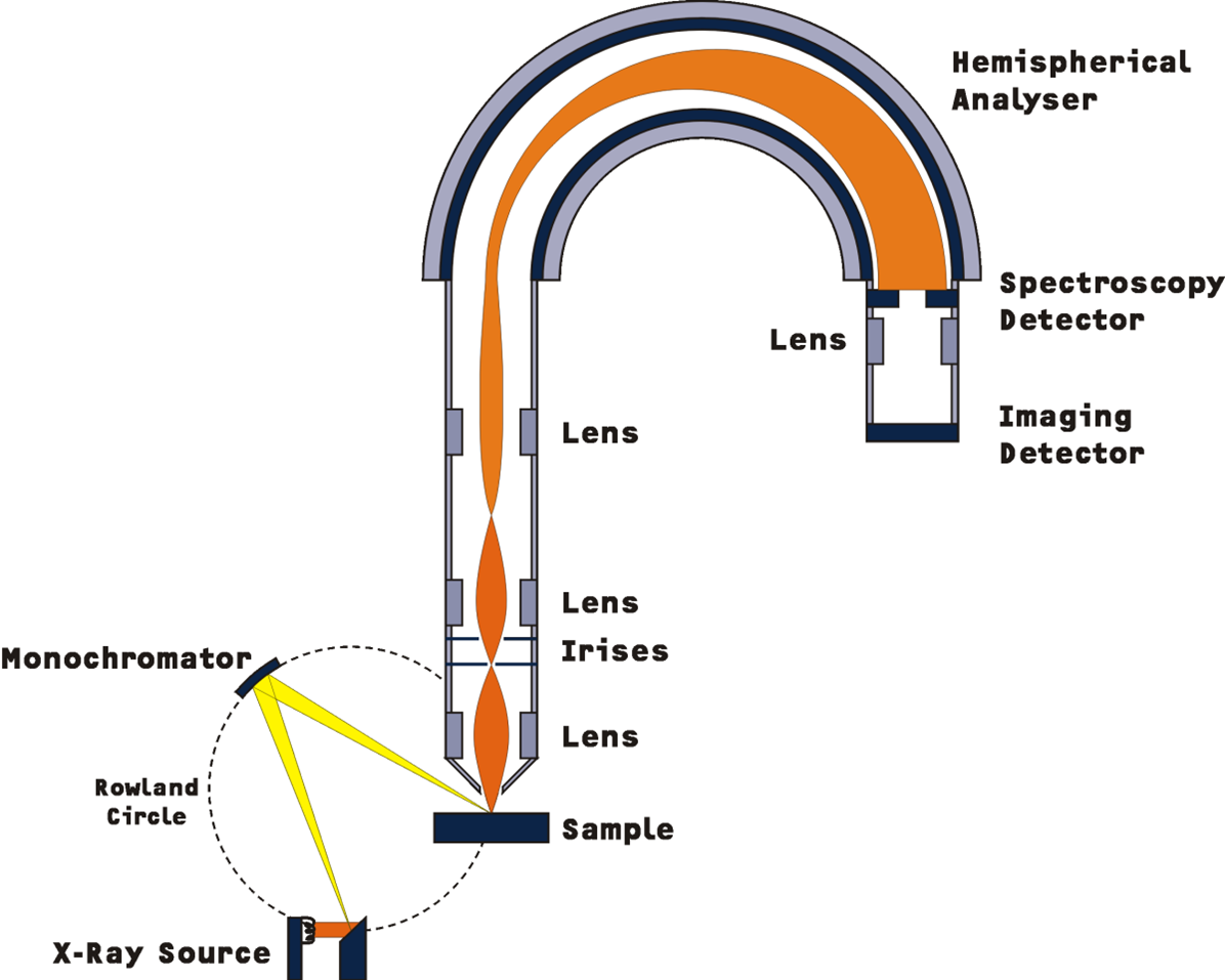
To ensure a constant energy resolution across the entire spectrum, the pass energy of the spectrometer remains constant for the complete spectrum. The kinetic energy of the incoming electrons is adjusted accordingly at the entrance of the spectrometer to measure the entire spectrum. The measuring of various photoelectron energies is therefore realised by applying a variable electrostatic field at the input of the analyser.
Depth information in XPS analysis

The angular dependence of the XPS signal allows the analysis of the depth distribution of elements or binding states near the surface (typically in the top 10 nm of the sample).
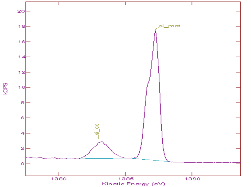
A typical example of this method is the determination of the layer thickness of oxide layers of silicon or aluminium for example. The following figure shows the aluminium 2p peak of aluminium foil. At 73.7 eV the signal of metallic aluminium can be recognised. At 75.4 eV the signal of the overlying oxide layer, means the oxidized metal, is present.
Based on the intensity ratio of these two lines a layer thickness of 4.9 nm can be estimated. At the same time the oxide / hydroxide ratio can be specified and possible contaminations can be detected.
Sputter depth profile measurements

Is element information required from a greater depth, sputter depth profile measurements are a useful method for gathering this information. In this method, the sample surface is removed layer by layer by means of accelerated ions (usually 3 kV Ar+). After each of these sputtering steps, the composition of the surface by XPS is reanalysed. Knowing the sputter rates of the sample material, the depth composition of the surface can be measured. An example of this technique shows the following picture.
Here the composition of the surface of a commercially available hard disk is measured. As a result, the layer structure can be reconstructed quantitatively.