

Purpose and strength of the technique
- Precise and rapid high-Resolution Imaging
- Very good depth of Focus
- Very flexible microscopy technique
- In combination with EDS (local) identification of elements
Technical Data
- Lateral Resolution: down to 0,8 nm
- Detectable Signals: Secondary electrons, back scattered electrons, X-rays
- Information depth: According to the operating Parameters from several Nanometers up to some micron.
- Excitation Energy: Low Voltage SEM: 10 V up to 1 kV, Standard SEM: 1 kV up to 30 kV
- Microscopyical analysis with Resolution down to the nanometer scale
- Texture and microstructure analysis of materials
- Measuring the morphological structure of porous materials
- Elemental microanalysis and (automated) particle characterization
- Identification of (inorganic) foreign material on product surfaces or in inclusions
- Chemical imaging of material distributions (e.g. of pharmaceuticals)
- Physical and chemical characterization of multi-layer thin films (cross section)
- Investigation of ageing, corrosion or oxidation of surfaces
- Failure analysis in delamination problems
- Investigation of joining problems in glueing, soldering, brazing or welding
- Determining the cause for electrical contact failures
- Quantitative analysis of the composition of small particles
Scanning Electron Microscopy (SEM) is used for high resolution imaging of a wide variety of different samples. Its great advantage is the enormous lateral resolution and the big depth of focus. Combined with an appropriate sample preparation this gives a detailed view into the morphology of surfaces, the structure of materials as well as biological specimens.
Principle of Operation
While a fine focussed electron beam scans a surface, several detectors register the products of the interaction processes between the electron beam and the sample. Their output signals are amplified and produce the image of the sample surface. For very thin samples the same principle can be used in transmission mode. This is called Scanning Transmission Electron Microscope (STEM).
Kinds of signals
The interaction between the primary electron beam and the sample leads to several interaction products such as secondary electrons (SE), back scattered electrons (BSE), Auger electrons (AE), light (cathodoluminescence), heat, and X-rays which are used for EDS analysis. This gives additionally information about the chemical composition of the sample.
Secondary electron images
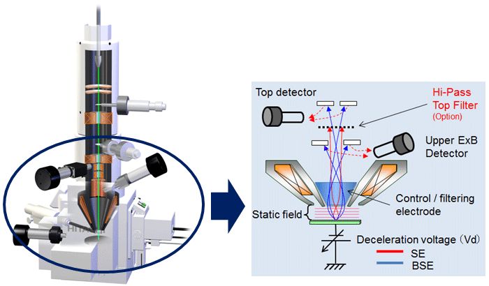
The most popular and thus well-known SEM images are generated by signals of secondary electron detectors. They detect these slow electrons whose kinetic energy is per definition below 50 eV. Two kinds of these detectors are widespread: Everhart-Thornley-detector inside the specimen chamber and InLense-detector inside the electron column.
Due to the very low kinetic energy of the secondary electrons their depth of information is just several nanometres since the SE which are produced in deeper regions inside the sample are not able to get out of it. Thus these secondary electron images show mostly the surface topography. The lateral resolution is dominated by the diameter of the primary electron beam. Modern field emission guns are able to produce beam diameters in the range of 1 nm while older tungsten hairpin guns give several 10 nm.
The contrast mechanisms are different to light microscopy. Edges are brighter than plains; plains tilted towards the detector are brighter than the far sides. These effects give the impression that the sample is viewed by the direction of the primary electron beam but illuminated by the detector as the light source.
The higher the atomic number of the sample components the brighter they appear also in SE images, because not only the primary electron beam produces secondary electrons but also the backscattered electrons do.
Back scattered electron images
Primary electrons which are scattered back by the sample are called back scattered electrons. Their kinetic energy is normally much higher than this of secondary electrons since it reaches nearly the kinetic energy of the primary electrons which is usually in the range of several keV. The intensity of the BSE electrons and thus the brightness of the BSE image is mostly determined by the mean atomic number of the sample. The higher the mean atomic number the brighter the image.
This is why these images are called material contrast images. They show the distribution of different materials / chemical elements within the sample. While Robinson-detectors show also topography contrast, semiconductor detectors are able to switch between material and topography contrast due to logical combination of single detector segments. Thus the interpretation of BSE images sometimes needs experience and caution.
X-ray microanalysis (EDS)
The detection of the X-rays which are emitted by the sample under electron bombardment gives quantitative information about the chemical composition of the sample. Details are available on the page about X-ray microanalysis (EDS).
Samples and sample preparation

All SEM images are taken under vacuum conditions. Thus the sample needs to be stable in a light to high vacuum.
Electrical isolators challenge the imaging since the primary electrons are nothing else than electric current. To overcome this problem the samples can either be imaged at low voltage conditions (around 1 keV) or coated with an electric conductive material such as noble metal (silver, gold, platinum) or carbon (graphite).